Multi-Wave Liquid Crystal Variable Retarder with Integrated Controller
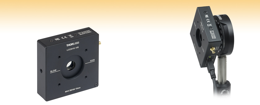
- Designed for Visible Light: 400 - 700 nm
- Variable Retardance of 0 - 4000 nm
- Externally Controllable, Programmable Retardance Sequences
LCC2415-VIS
Application Idea
LCC2415-VIS Variable Retarder Connected to an RSP1 Rotation Mount with an SM1T2 Lens Tube Coupler

Please Wait
Operating Principle
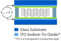
High Retardance
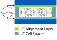
Low Retardance
In their nematic phase, liquid crystal molecules have an ordered orientation, which together with the stretched shape of the molecules creates an optical anisotropy. When an electric field is applied, the molecules align to the field and the level of birefringence is controlled by the tilting of the LC molecules.
| Selection Guide for LC Retarders | |
|---|---|
| Type | Clear Aperture |
| Half Wave | Ø10 mm or Ø20 mm |
| Half Wave, Thermally Stabilized | Ø10 mm |
| Full Wave | Ø10 mm or Ø20 mm |
| Full Wave, Thermally Stabilized | Ø20 mm |
| Multi-Wave | Ø10 mm |
| Multi-Wave, Integrated Controller | Ø10 mm |
| Custom LC Retarders | |
Features
- Nematic Liquid Crystal Wave Plates with Variable, Computer-Controlled Retardance
- Retardance Range: 0 - 4000 nm (True Zero to 6.32λ at 633 nm)
- Designed for Input Wavelengths in the 400 - 700 nm Range
- Ø10 mm Clear Aperture
- Powered over USB; Communicates with Computer via USB or Bluetooth® Using Included Software
- SMC Trigger-In Enables User-Defined Retardance Sequences (See Software Tab; SMC Cable Not Included)
- Several Mounting Options
- Internal SM1 (1.035"-40) Threads on Both Sides for Ø1" Lens Tubes
- Four 4-40 Tapped Holes on Both Sides for 30 mm Cage Systems
- Two 8-32 (M4) Tapped Holes for Ø1/2" Post Mounting
Designed for the visible wavelength range (400 - 700 nm), this Multi-Wave Liquid Crystal Variable Retarder offers an absolute retardance that can be continuously varied from 0 to 4000 nm, corresponding to a maximum possible retardance of 5.71λ at 700 nm and 10λ at 400 nm. The retardance magnitude is controlled by applying a voltage to an LC cell, shown schematically in the Operating Principle box to the right. Because this wave plate contains no moving parts, it is able to achieve switching times on the order of hundreds of milliseconds, as shown in the Performance tab.
The included Windows® software package allows the user to set the retardance (in units of waves, degrees, or nm) or the voltage across the liquid crystal cell (0 V to 10 V, with 0.2 mV resolution). For retardance sequences, the user needs to supply an external trigger signal (5 V TTL) through the female SMC connector on the housing (see photo below) to advance from step to step; the step will occur on the falling edge of the TTL signal. An SMC cable, sold separately, is required to trigger a sequence.
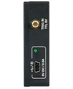
Click to Enlarge
USB and SMC Connectors on the Side of LCC2415-VIS Retarder
This variable wave plate has a clear aperture of Ø10 mm, and it is contained in a compact 60.0 mm x 60.0 mm x 18.0 mm (2.36" x 2.36" x 0.71") housing for simple integration into an optical setup. The housing incorporates both the liquid crystal (LC) cell and the controller, so no other external boxes need to be placed onto the tabletop. For mounting, the housing contains internal SM1 (1.035"-40) threads on both sides for our Ø1" lens tubes, four 4-40 taps on both sides for our 30 mm cage systems, and two 8-32 (M4) taps for Ø1/2" posts.
Computer Control
The retarder communicates with a Windows computer using either a wired USB connection (via the included mini-USB cable) or a wireless Bluetooth® connection. To use wireless functionality, the PC requires a Bluetooth controller, which is not included. Also note that when using Bluetooth, a USB connection is still required to power the device. A high-quality external USB charger (5 VDC, 0.5 A max) may be used to power the device.
Alignment
The retarder is designed to provide variable phase modulation for linearly polarized input light. For optimal performance, this light should be polarized at 45° with respect to the slow axis of the retarder. In order to achieve the correct alignment, we recommend using the SM1T2 Lens Tube Coupler to attach the retarder to an SM1-threaded rotation mount. An example configuration is pictured in the image at the top of the page.
The Bluetooth® word mark is a registered trademark owned by Bluetooth SIG, Inc. and any use of such marks is under license.
| Item # | LCC2415-VIS(/M) | ||
|---|---|---|---|
| Optical Specifications | |||
| Wavelength Range | 400 - 700 nm | ||
| Wavelength Input Resolutiona | 5 nm | ||
| Retardance Range | 0 - 4000 nm | ||
| Retardance Resolution | 1 nm | ||
| Retardance Accuracyb | ±1% | ||
| Clear Aperture | Ø10 mm | ||
| Retardance Uniformity | <λ/50 (RMS) over the Entire Clear Aperture | ||
| Wavefront Distortion | ≤λ/4 at 635 nm | ||
| Surface Quality | 40-20 Scratch-Dig | ||
| Damage Thresholds | Pulsed (ns) | 1.0 J/cm2 (532 nm, 10 Hz, 8 ns, Ø200 µm) | |
| Pulsed (fs) | 0.01 J/cm2 (532 nm, 100 Hz, 76 fs, Ø162 µm) | ||
| Electrical Specifications | |||
| Trigger Connector | SMC | ||
| Trigger Input | 5 V TTL | ||
| Drive Voltage Range | 0 - 10 VRMS | ||
| Drive Voltage Resolutionc | 0.2 mV | ||
| Power | Mini-USB (5 VDC, 0.5 A Max) | ||
| Physical Specifications | |||
| Housing Dimensions | 60.0 mm x 60.0 mm x 18.0 mm (2.36" x 2.36" x 0.71") |
||
| Operating Temperatured | 0 to 70 °C | ||
| Calibration Temperatureb | 20 to 30 °C | ||
| Storage Temperature | -15 to 70 °C | ||
| Weight | 100 g | ||
| Liquid Crystal Material | Nematic Liquid Crystal | ||
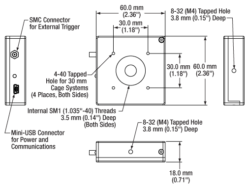
Mechanical Drawing of LCC2415-VIS(/M)
Graphs
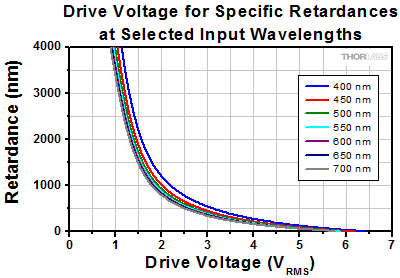
These plots were obtained using a typical retarder unit; the actual performance will vary from unit to unit. All units are factory calibrated before shipment so that they will provide retardance of 0 nm to 4000 nm (±1%) for input wavelengths in the 400 - 700 nm range when operated from the included software. The unit-specific calibration data is available upon request.
All performance data was taken at normal incidence at an ambient temperature of 25 °C.
Click to Enlarge
Click for Raw Data at 5 nm Increments in the 400 - 700 nm Range
This plot shows the drive voltage, VRMS, that the software applies to the liquid crystal cell to achieve the desired retardance magnitude.
Click to Enlarge
Click for Raw Data
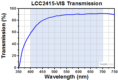
The shaded region in this plot indicates the LCC2415-VIS's design wavelength range.
Click to Enlarge
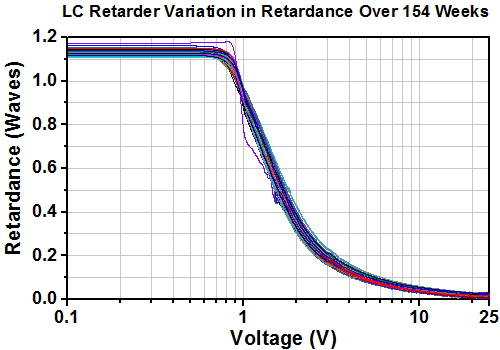
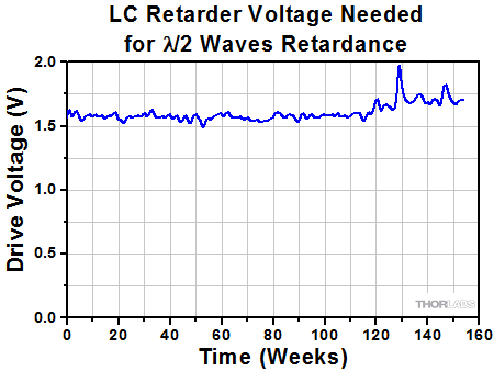
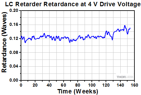
Graph shows variation in retardance over a period of 154 weeks.
Long-Term Stability
Our liquid crystal retarders exhibit consistent performance over time. The graph to the right shows the retardance vs. voltage for one previous-generation LCC1112-A three-quarter wave retarder, driven by our LCC25 liquid crystal controller over 154 weeks. The retardance was tested once per week and varied only slightly over the testing period. For the complete set of data from testing each week, please click below to download the full data file.
The graph below to the left shows that the retardance varies only slightly at a constant voltage, while the graph below to the right shows that the voltage varies only slightly at a constant retardance. Similar consistency in performance can also be expected for our other models of retarders. To maximize the long-term stability of our retarders, we recommend always using the LCC25 controller. It is specifically designed to reduce the DC voltage offset, thus minimizing charge buildup and maximizing stability.
Click Here to Download Long-Term Performance Data
Switching Time
Liquid crystal (LC) retarders feature a short switching time compared to mechanical variable wave plates due to the lack of moving parts. The switching time of a liquid crystal retarder depends on several variables, some of which are controlled in the manufacturing process, and some of which are controlled by the user.
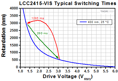
In general, liquid crystal retarders will always switch faster when changing from a high to a low birefringence value. Additionally, the higher the operating temperature is, the faster the retarder will switch from one state to another due to the decreased viscosity at the higher temperature. The LCC2415-VIS retarder is designed to work at temperatures up to 70 °C.
For any given retarder, the switching speed will always be faster at higher voltages. If faster switching speeds are desired, we recommend using the retarder together with a fixed wave plate so that the retarder can be used at a larger voltage.
The switching speed is also directly proportional to the thickness of the LC retarder, the rotational viscosity of the LC material, and the dielectric anisotropy of the LC material. However, since each of those variables affects other operating parameters as well, our LC retarders are designed to optimize overall performance, with a special emphasis on switching time. We also offer custom and OEM LC retarders optimized for other parameters, as well as faster liquid crystal retarders. See the Custom Capabilities tab above, or contact techsupport@thorlabs.com for details.
| Sample Switching Times at Various Temperatures | ||
|---|---|---|
| Temperature | Rise Time (Increasing Retardance) |
Fall Time (Decreasing Retardance) |
| From 3.1 VRMS to 1.92 VRMS | ||
| 25 °C | 867.5 ms | 252.5 ms |
| 45 °C | 495 ms | 37.5 ms |
| 60 °C | 495 ms | 87.5 ms |
| 70 °C | 330 ms | 77.5 ms |
| From 3.1 VRMS to 1.34 VRMS | ||
| 25 °C | 1285 ms | 280 ms |
| 45 °C | 675.5 ms | 135 ms |
| 60 °C | 735 ms | 115 ms |
| 70 °C | 837.5 ms | 92.5 ms |
| From 3.1 VRMS to 1.04 VRMS | ||
| 25 °C | 3530 ms | 450 ms |
| 45 °C | 1710 ms | 162 ms |
| 60 °C | 2270 ms | 135 ms |
| 70 °C | 1755 ms | 145 ms |
Click to Enlarge
This plot gives switching times of our LCC2415-VIS retarder at 25 °C for V1 = 3.1 VRMS and V2 = 1.34 VRMS. At an input wavelength of 400 nm, these drive voltages produce a retardance of 505 nm and 2835 nm, respectively. The rise time is greater than the fall time, meaning that a retardance increase takes longer than the equivalent retardance decrease.
Software for the LCC2415-VIS Multi-Wave Variable Retarder with Integrated Controller
Click to Enlarge
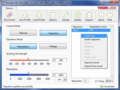
Main Window of LCC2415-VIS User Interface
Software
Version 1.1.0
GUI interface for controlling the multi-wave variable retarder via a PC, as well as C/C++ code examples and LabVIEW VIs. To download, click the button below.
This software also requires the LabVIEW 2011 Runtime Engine, which is available from www.ni.com.
GUI Interface
Our Windows® interface provides access to all of the settings of our multi-wave variable retarders. To change the retardance imparted by the LCC2415-VIS, the user can enter either an absolute retardation (in nm) or a relative retardation (in waves or degrees). Alternatively, the user may enter the actual voltage applied to the liquid crystal cell (from 0 V to 10 V, with 1 mV resolution).
The GUI also allows easy entry of user-defined retardance sequences, as shown in the screenshot to the right. A sequence consists of a number of steps, each of which has its own retardation value. In addition to manual entry, the software allows sequences to be defined by a starting value, an ending value, and the step size between start and end. Sequences can also be imported from and exported to CSV format.
Once the sequence is entered, the user needs to supply an external trigger signal (5 V TTL) through the female SMC connector on the housing to advance from step to step; the step will occur on the falling edge of the TTL signal. SMC cables are sold separately.
Custom Software Development
We also provide C/C++ and LabVIEW software development kits for controlling the LCC2415-VIS with other instruments. Sample C++ code and LabVIEW programs help to illustrate how the C commands and LabVIEW VIs can be utilized. Full documentation on the available commands is provided in the manual.
The liquid crystal (LC) cells used in Thorlabs' liquid crystal retarders consist of a transparent cell filled with a solution of liquid crystal molecules. Two parallel faces of the cell wall are coated with a transparent conductive film so that a voltage can be applied across the cell.
As shown in the pictures to the right, in the absence of an applied voltage, the orientation of the LC molecules is determined by the alignment layer that is created by the organic polyimide coating and rubbing angle. The molecules' orientation, together with the stretched shape of the molecules, creates the birefringence necessary for retardance. The retardance, δ, in units of wavenumbers, is given by the following formula:

Here, d is the effective path length through the liquid crystal solution, λ is the wavelength, and Δn is the difference in the refractive index between the parallel and perpendicular polarization directions.
When an AC voltage is applied across the cell, the molecules will change from their default orientation and align to the applied electric field. The level of birefringence is determined by the tilting of the LC molecules and controlled by the VRMS magnitude. Hence, the phase of a linearly polarized beam of light can be actively modulated by varying the applied voltage.
It is important to note that the LC molecules adjacent to the alignment layer (shown in green in the pictures above) do not respond to the applied field, preventing the retardance imparted by the LC cell from being truly zero. Hence, we have included an extra, fixed-retardance wave plate in the construction of the LCC2415-VIS, which compensates for the retardation imparted by the non-moving LC molecules.
| Damage Threshold Specifications | |
|---|---|
| Laser Type | Damage Threshold |
| Pulsed (ns) | 1.0 J/cm2 (532 nm, 10 Hz, 8 ns, Ø200 µm) |
| Pulsed (fs) | 0.01 J/cm2 (532 nm, 100 Hz, 76 fs, Ø162 µm) |
Damage Threshold Data
The specifications to the right are measured data for Thorlabs' LCC2415-VIS Liquid Crystal Retarder.
Laser Induced Damage Threshold Tutorial
The following is a general overview of how laser induced damage thresholds are measured and how the values may be utilized in determining the appropriateness of an optic for a given application. When choosing optics, it is important to understand the Laser Induced Damage Threshold (LIDT) of the optics being used. The LIDT for an optic greatly depends on the type of laser you are using. Continuous wave (CW) lasers typically cause damage from thermal effects (absorption either in the coating or in the substrate). Pulsed lasers, on the other hand, often strip electrons from the lattice structure of an optic before causing thermal damage. Note that the guideline presented here assumes room temperature operation and optics in new condition (i.e., within scratch-dig spec, surface free of contamination, etc.). Because dust or other particles on the surface of an optic can cause damage at lower thresholds, we recommend keeping surfaces clean and free of debris. For more information on cleaning optics, please see our Optics Cleaning tutorial.
Testing Method
Thorlabs' LIDT testing is done in compliance with ISO/DIS 11254 and ISO 21254 specifications.
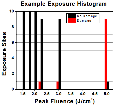
First, a low-power/energy beam is directed to the optic under test. The optic is exposed in 10 locations to this laser beam for 30 seconds (CW) or for a number of pulses (pulse repetition frequency specified). After exposure, the optic is examined by a microscope (~100X magnification) for any visible damage. The number of locations that are damaged at a particular power/energy level is recorded. Next, the power/energy is either increased or decreased and the optic is exposed at 10 new locations. This process is repeated until damage is observed. The damage threshold is then assigned to be the highest power/energy that the optic can withstand without causing damage. A histogram such as that below represents the testing of one BB1-E02 mirror.
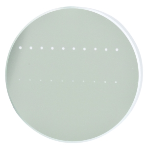
The photograph above is a protected aluminum-coated mirror after LIDT testing. In this particular test, it handled 0.43 J/cm2 (1064 nm, 10 ns pulse, 10 Hz, Ø1.000 mm) before damage.
| Example Test Data | |||
|---|---|---|---|
| Fluence | # of Tested Locations | Locations with Damage | Locations Without Damage |
| 1.50 J/cm2 | 10 | 0 | 10 |
| 1.75 J/cm2 | 10 | 0 | 10 |
| 2.00 J/cm2 | 10 | 0 | 10 |
| 2.25 J/cm2 | 10 | 1 | 9 |
| 3.00 J/cm2 | 10 | 1 | 9 |
| 5.00 J/cm2 | 10 | 9 | 1 |
According to the test, the damage threshold of the mirror was 2.00 J/cm2 (532 nm, 10 ns pulse, 10 Hz, Ø0.803 mm). Please keep in mind that these tests are performed on clean optics, as dirt and contamination can significantly lower the damage threshold of a component. While the test results are only representative of one coating run, Thorlabs specifies damage threshold values that account for coating variances.
Continuous Wave and Long-Pulse Lasers
When an optic is damaged by a continuous wave (CW) laser, it is usually due to the melting of the surface as a result of absorbing the laser's energy or damage to the optical coating (antireflection) [1]. Pulsed lasers with pulse lengths longer than 1 µs can be treated as CW lasers for LIDT discussions.
When pulse lengths are between 1 ns and 1 µs, laser-induced damage can occur either because of absorption or a dielectric breakdown (therefore, a user must check both CW and pulsed LIDT). Absorption is either due to an intrinsic property of the optic or due to surface irregularities; thus LIDT values are only valid for optics meeting or exceeding the surface quality specifications given by a manufacturer. While many optics can handle high power CW lasers, cemented (e.g., achromatic doublets) or highly absorptive (e.g., ND filters) optics tend to have lower CW damage thresholds. These lower thresholds are due to absorption or scattering in the cement or metal coating.
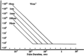
LIDT in linear power density vs. pulse length and spot size. For long pulses to CW, linear power density becomes a constant with spot size. This graph was obtained from [1].
Pulsed lasers with high pulse repetition frequencies (PRF) may behave similarly to CW beams. Unfortunately, this is highly dependent on factors such as absorption and thermal diffusivity, so there is no reliable method for determining when a high PRF laser will damage an optic due to thermal effects. For beams with a high PRF both the average and peak powers must be compared to the equivalent CW power. Additionally, for highly transparent materials, there is little to no drop in the LIDT with increasing PRF.
In order to use the specified CW damage threshold of an optic, it is necessary to know the following:
- Wavelength of your laser
- Beam diameter of your beam (1/e2)
- Approximate intensity profile of your beam (e.g., Gaussian)
- Linear power density of your beam (total power divided by 1/e2 beam diameter)
Thorlabs expresses LIDT for CW lasers as a linear power density measured in W/cm. In this regime, the LIDT given as a linear power density can be applied to any beam diameter; one does not need to compute an adjusted LIDT to adjust for changes in spot size, as demonstrated by the graph to the right. Average linear power density can be calculated using the equation below.

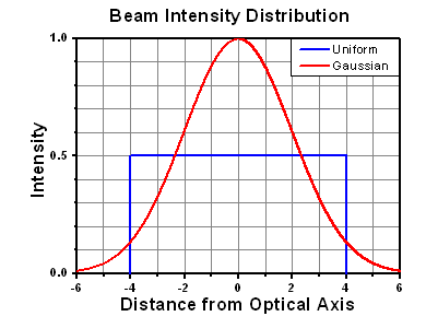
The calculation above assumes a uniform beam intensity profile. You must now consider hotspots in the beam or other non-uniform intensity profiles and roughly calculate a maximum power density. For reference, a Gaussian beam typically has a maximum power density that is twice that of the uniform beam (see lower right).
Now compare the maximum power density to that which is specified as the LIDT for the optic. If the optic was tested at a wavelength other than your operating wavelength, the damage threshold must be scaled appropriately. A good rule of thumb is that the damage threshold has a linear relationship with wavelength such that as you move to shorter wavelengths, the damage threshold decreases (i.e., a LIDT of 10 W/cm at 1310 nm scales to 5 W/cm at 655 nm):

While this rule of thumb provides a general trend, it is not a quantitative analysis of LIDT vs wavelength. In CW applications, for instance, damage scales more strongly with absorption in the coating and substrate, which does not necessarily scale well with wavelength. While the above procedure provides a good rule of thumb for LIDT values, please contact Tech Support if your wavelength is different from the specified LIDT wavelength. If your power density is less than the adjusted LIDT of the optic, then the optic should work for your application.
Please note that we have a buffer built in between the specified damage thresholds online and the tests which we have done, which accommodates variation between batches. Upon request, we can provide individual test information and a testing certificate. The damage analysis will be carried out on a similar optic (customer's optic will not be damaged). Testing may result in additional costs or lead times. Contact Tech Support for more information.
Pulsed Lasers
As previously stated, pulsed lasers typically induce a different type of damage to the optic than CW lasers. Pulsed lasers often do not heat the optic enough to damage it; instead, pulsed lasers produce strong electric fields capable of inducing dielectric breakdown in the material. Unfortunately, it can be very difficult to compare the LIDT specification of an optic to your laser. There are multiple regimes in which a pulsed laser can damage an optic and this is based on the laser's pulse length. The highlighted columns in the table below outline the relevant pulse lengths for our specified LIDT values.
Pulses shorter than 10-9 s cannot be compared to our specified LIDT values with much reliability. In this ultra-short-pulse regime various mechanics, such as multiphoton-avalanche ionization, take over as the predominate damage mechanism [2]. In contrast, pulses between 10-7 s and 10-4 s may cause damage to an optic either because of dielectric breakdown or thermal effects. This means that both CW and pulsed damage thresholds must be compared to the laser beam to determine whether the optic is suitable for your application.
| Pulse Duration | t < 10-9 s | 10-9 < t < 10-7 s | 10-7 < t < 10-4 s | t > 10-4 s |
|---|---|---|---|---|
| Damage Mechanism | Avalanche Ionization | Dielectric Breakdown | Dielectric Breakdown or Thermal | Thermal |
| Relevant Damage Specification | No Comparison (See Above) | Pulsed | Pulsed and CW | CW |
When comparing an LIDT specified for a pulsed laser to your laser, it is essential to know the following:
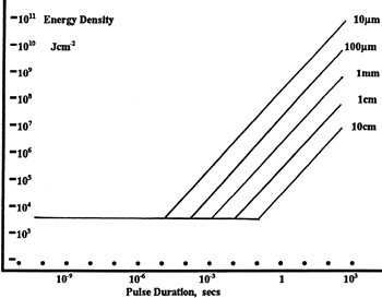
LIDT in energy density vs. pulse length and spot size. For short pulses, energy density becomes a constant with spot size. This graph was obtained from [1].
- Wavelength of your laser
- Energy density of your beam (total energy divided by 1/e2 area)
- Pulse length of your laser
- Pulse repetition frequency (prf) of your laser
- Beam diameter of your laser (1/e2 )
- Approximate intensity profile of your beam (e.g., Gaussian)
The energy density of your beam should be calculated in terms of J/cm2. The graph to the right shows why expressing the LIDT as an energy density provides the best metric for short pulse sources. In this regime, the LIDT given as an energy density can be applied to any beam diameter; one does not need to compute an adjusted LIDT to adjust for changes in spot size. This calculation assumes a uniform beam intensity profile. You must now adjust this energy density to account for hotspots or other nonuniform intensity profiles and roughly calculate a maximum energy density. For reference a Gaussian beam typically has a maximum energy density that is twice that of the 1/e2 beam.
Now compare the maximum energy density to that which is specified as the LIDT for the optic. If the optic was tested at a wavelength other than your operating wavelength, the damage threshold must be scaled appropriately [3]. A good rule of thumb is that the damage threshold has an inverse square root relationship with wavelength such that as you move to shorter wavelengths, the damage threshold decreases (i.e., a LIDT of 1 J/cm2 at 1064 nm scales to 0.7 J/cm2 at 532 nm):

You now have a wavelength-adjusted energy density, which you will use in the following step.
Beam diameter is also important to know when comparing damage thresholds. While the LIDT, when expressed in units of J/cm², scales independently of spot size; large beam sizes are more likely to illuminate a larger number of defects which can lead to greater variances in the LIDT [4]. For data presented here, a <1 mm beam size was used to measure the LIDT. For beams sizes greater than 5 mm, the LIDT (J/cm2) will not scale independently of beam diameter due to the larger size beam exposing more defects.
The pulse length must now be compensated for. The longer the pulse duration, the more energy the optic can handle. For pulse widths between 1 - 100 ns, an approximation is as follows:

Use this formula to calculate the Adjusted LIDT for an optic based on your pulse length. If your maximum energy density is less than this adjusted LIDT maximum energy density, then the optic should be suitable for your application. Keep in mind that this calculation is only used for pulses between 10-9 s and 10-7 s. For pulses between 10-7 s and 10-4 s, the CW LIDT must also be checked before deeming the optic appropriate for your application.
Please note that we have a buffer built in between the specified damage thresholds online and the tests which we have done, which accommodates variation between batches. Upon request, we can provide individual test information and a testing certificate. Contact Tech Support for more information.
[1] R. M. Wood, Optics and Laser Tech. 29, 517 (1998).
[2] Roger M. Wood, Laser-Induced Damage of Optical Materials (Institute of Physics Publishing, Philadelphia, PA, 2003).
[3] C. W. Carr et al., Phys. Rev. Lett. 91, 127402 (2003).
[4] N. Bloembergen, Appl. Opt. 12, 661 (1973).
Thorlabs' Custom Liquid Crystal Capabilities
Thorlabs offers a large variety of liquid crystal (LC) retarders from stock, including half-, three-quarter-, and full-wave models with a Ø10 mm or Ø20 mm clear aperture as well as half-wave temperature-controlled models. However, we also offer OEM and custom retarders. The retardance range, coating, rubbing angle, temperature stabilization, and size can be customized to meet many unique optical designs. We also offer other custom liquid crystal devices, such as empty LC cells, polarizaton rotators, and noise eaters. For more information about ordering a custom liquid crystal device, please contact Thorlabs' technical support.
Our engineers work directly with our customers to discuss the specifications and other design aspects of a custom liquid crystal retarder. They will analyze both the design and feasibility to ensure the custom products are manufactured to high-quality standards and in a timely manner.
Polyimide (PI) Coating and Rubbing - Custom Alignment Angle
In their nematic phase, liquid crystal molecules naturally align to an average orientation, which together with their stretched shape creates an optical anisotropy, or direction-dependent optical effect. The orientation of the LC molecules in an LC cell, in the absence of an applied voltage, is determined by the alignment layer, which is created by the polyimide (PI) coating and rubbing at a specific angle. Rubbing creates grooves which the liquid crystal molecules will align to. Users can choose any initial orientation of LC molecules by specifying the rubbing angle.
Custom Cell Spacing
The wall spacing inside of the liquid crystal cell, which determines the thickness of LC material, can be customized during the manufacturing process. The retardance range of an LC cell is dependent on the LC material thickness:
![]()
Here, δ is the retardance in waves, d is the thickness of the LC material, λν is the wavelength of light, and Δn is the birefringence of the LC material used. Thus, for a given wavelength, the retardance is determined by the wall spacing inside the LC cell (i.e., the thickness of the LC layer). We offer standard retardance ranges of λ/2 to 30 nm, 3λ/4 to 30 nm, and λ to 30 nm, but higher retardance ranges may also be ordered.
Custom Liquid Crystal Material
Customers can also provide their own liquid crystal material, and Thorlabs will use it to fill the liquid crystal cell. Since different liquid crystal materials have different birefringence values, varying the material enables a different retardance range.
Temperature Control / Switching Time
A temperature sensor can also be integrated into the LC variable retarder. Using a temperature controller, the temperature of the retarder can be actively stabilized to within ±0.1 °C. The viscosity of the liquid crystal material is lowered at higher temperatures, allowing the retarder to switch from one state to another due to the decreased viscosity. An active temperature control system can be used to heat the retarder, allowing it to operate at higher switching speeds.
Assembly / Housing
If desired, we can manufacture custom liquid crystal retarders without housings.
Testing
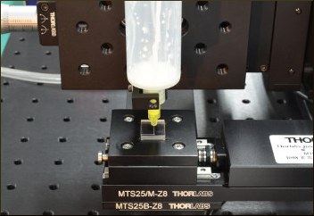
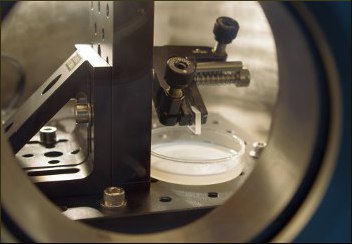
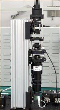
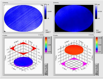
Each LC retarder is tested for birefringence, uniformity, and fast axis angle, using the measurement setup shown in the photo to the left. The equipment measures the 2-dimensional birefringence distribution using wave plates and a CCD camera. The image to the right shows a sample test result of a liquid crystal retarder, showing excellent uniformity.
For More Information
Contact Thorlabs' technical support for more information about our custom liquid crystal device options or to place an order.
| Custom Capability | Custom Specification |
|---|---|
| Patterned Retarder Size | Ø100 µm to Ø2" |
| Patterned Retarder Shape | Any |
| Microretarder Size | ≥Ø30 µm |
| Microretarder Shape | Round or Square |
| Retardance Range @ 632.8 nm | 50 to 550 nm |
| Substrate | N-BK7, UV Fused Silica, or Other Glass |
| Substrate Size | Ø5 mm to Ø2" |
| AR Coating | -A: 350 - 700 nm -B: 650 - 1050 nm -C: 1050 - 1700 nm |

Click to Enlarge
Figure 97A Patterned Retarder with Random Distribution
Features
- Build a Custom Microretarder
- Customize Size, Shape, and Substrate Material
- Retardance Range: 50 - 550 nm
- Fast Axis Resolution: <1º
- Retardance Fluctuations Under 30 nm
Applications
- 3D Displays
- Polarization Imaging
- Diffractive Optical Applications: Polarization Gratings, Polarimetry, and Beam Steering
Thorlabs offers customizable patterned retarders, available in any pattern size from Ø100 µm to Ø2" and any substrate size from Ø5 mm to Ø2". These custom retarders are composed of an array of microretarders, each of which has a fast axis aligned to a different angle than its neighbor. The size and shape of the microretarders are also customizable. They can be as small as 30 µm and in shapes including circles and squares. This control over size and shape of the individual microretarders allows us to construct a large array of various patterned retarders to meet nearly any experimental or device need.
These patterned retarders are constructed from our liquid crystals and liquid crystal polymers. Using photo alignment technology, we can secure the fast axis of each microretarder to any angle within a resolution of <1°. Figures 97A, 97B, and 97C show examples of our patterned retarders. The figures represent measured results of the patterned retarder captured on an imaging polarimeter and demonstrate that the fast axis orientation of any one individual microretarder can be controlled deterministically and separately from its neighbors.
The manufacturing process for our patterned retarders is controlled completely in house. It begins by preparing the substrate, which is typically N-BK7 or UV fused silica (although other glass substrates may be compatible as well). The substrate is then coated with a layer of photoalignment material and placed in our patterned retarder system where sections are exposed to linearly polarized light to set the fast axis of a microretarder. The area of the exposed sections depends on the desired size of the microretarder; the fast axis can be set between 0° and 180° with a resolution <1°. Once set, the liquid crystal cell is constructed by coating the device with a liquid crystal polymer and curing it with UV light.
Thorlabs' LCP depolarizers provide one example of these patterned retarders. In principle, a truly randomized pattern may be used as a depolarizer, since it scrambles the input polarization spatially. However, such a pattern will also introduce a large amount of diffraction. For our depolarizers, we designed a linearly ramping fast axis angle and retardance that can depolarize both broadband and monochromatic beams down to diameters of 0.5 mm without introducing additional diffraction. For more details, see the webpage for our LCP depolarizers.
By supplying Thorlabs with a drawing of the desired patterned retarder or an excel file of the fast axis distribution, we can construct almost any patterned retarder. For more information on creating a patterned retarder, please contact Tech Support.

Click to Enlarge
Figure 97B Patterned Retarder with a Spiral Distribution

Click to Enlarge
Figure 97C Patterned Retarder with a Pictoral Distribution
| Posted Comments: | |
Bruce Kane
(posted 2024-07-29 12:40:36.467) Are the LC retarders you sell usable with CW sources? Or are there drift and stability issues that prevent this? Your specs seem to imply usage with pulsed or AC sources only. cdolbashian
(posted 2024-08-01 03:14:05.0) Thanks for contacting Thorlabs! Our LC retarders are usable with CW sources as well. The pulse-related specification in the spec sheet is only about the damage threshold. We will contact you directly to gather more information about your specific laser parameters and the feasibility of using it with our LC retarders. Raj Patel
(posted 2021-02-11 15:31:35.22) Is it possible to communicate with the device via serial commands instead of using dll? I would like to control the device via Matlab and serial communication seems easier than loading C libraries. Do you have examples of using serial commands to communicate with LCC2415? YLohia
(posted 2021-02-18 10:26:30.0) Thank you for contacting Thorlabs. The LCC2415-VIS can be controlled by a serial commands through the USB port or Bluetooth (please see Section 6 in the manual). The current SDK can support C/C++ and LabView but, unfortunately, and we haven't performed full test compatibility for Matlab (and thus don't have example for that environment). jouni.peltoniemi
(posted 2018-02-23 11:57:25.64) The view looks quite yellow and scratched.
As if there would be some cover to be removed, but I cannot get anything detached either. What to do? YLohia
(posted 2018-03-30 09:50:59.0) Response from Yashasvi at Thorlabs USA: Hello, thank you for contacting Thorlabs. The yellow tape (same as our part number KAP22-075) that you see is for dust protection; you will have to remove it in order to use the device correctly. You may need use tweezers when removing the tape to avoid damaging the optics on the unit. sebastien.loranger
(posted 2015-08-11 10:15:47.73) We were excited by this product considering the integrated controller, but were very disapointed upon using it. It is complicated to use because of the required trigger. Why not allow a triggering from the software?! Also, for your information, no one has SMC connectors in an optics labs... this is very irritating! You should at least give a BNC-SMC adapter with this product.
Regards,
Sébastien Loranger besembeson
(posted 2015-09-24 06:44:23.0) Response from Bweh at Thorlabs USA: We are planning to add the soft triggering function in software level. There is no timeline yet for this but when this is added, you will just need to download the new software from the website. I will contact you to provide the adapter if you still need it. |
 Products Home



 Multi-Wave LC Retarder, Integrated Controller